Kicad c++ walkthrough – footprint APIs
# return a list of modules in a library. Takes a library name:
mods = pcbnew.FootprintsInLib('MountingHole')
# Returns information about a footprint.
# The ':' delimiter between the library and modules is important.
pcbnew.FootprintInfo('MountingHole:MountingHole_3.2mm_M3')
# output:
{ 'uniquepadcount': 0, 'padcount': 0, 'name': 'MountingHole_3.2mm_M3',
 'lib': 'MountingHole', 'doc': 'Mounting Hole 3.2mm, no annular, M3',
 'ordernum': 0, 'keywords': 'mounting hole 3.2mm no annular m3'}") FootprintInfo;
# returns a list of all available footprint libraries
pcbnew.GetLogicalLibs;
Scripting fusion 360 designs into kicad
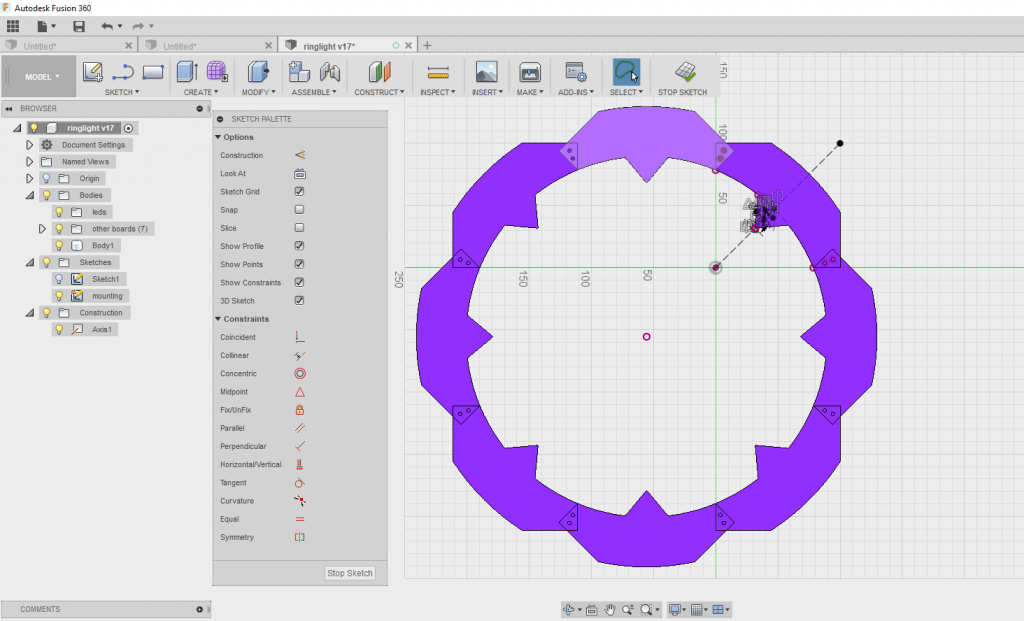
The layout of this board was designed in fusion 360 and brought into kicad via scripting. Very little manual work was required in pcbnew; it amounted mostly to deleting stuff and changing some zone names. The scripts also did the routing and placed the many vias
The code I demonstrate can be found on my git hub here and here.
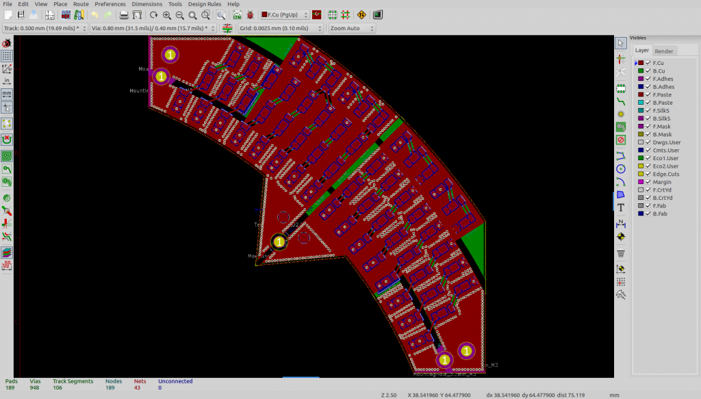
This board implements a ring light for photography (I use multiple boards to stay within the 10×10 limit of cheap fabricators:
I’ve created a video show all of the steps in kicad:
I won’t explain the code in this post, I’ll do that in future posts. I will, however, take a moment to recommend some useful python libraries:
The SciPy library is fantastic for graph algorithms like minimum spanning tree and delanay triangulation
The shapely library is very nice for polygon manipulation. Merging polygons, bloating and shrinking them…
The dxf_grabber library is how I parse dxf files. Together with shapely, you can do a lot of import stuff. 1
Hope it helps
sadly, I had already implemented a bunch of code merging lines and arcs into polygons.↩
Zones with holes from SVG
I’ve written about zones and boundaries before. Since then, the data structs behind zones have changed a bit. Also, I didn’t cover zones with holes. The old post is still relevant and there’s a bunch I won’t repeat here.
In this post, I talk about zones with holes and with multiple boundaries. Multiple boundaries makes it easier to move the zones together as a unit.
The code associated with this post is here.
Here’s a video talking mostly about the steps needed in inkscape to draw the graphic. Also has scripting details, but the text below is probably more informative:
Zone basics, revisited
pcbnew zones are stored in ZONE_CONTAINERs. They are what you get when you call board.InsertArea to create a new zone. Something like this:
[code]
SCALE = 1000000.0
zone_container = board.InsertArea(powernet.GetNet(), 0, powerlayer,
int(10*SCALE), int(10*SCALE),
pcbnew.CPolyLine.DIAGONAL_EDGE)
[/code]
That creates a single point zone on net powernet and layerpowernet1
To modify the zone, you need to access the shape_poly_set. It’s a single data struct that holds all of the coordinates.
[code]
shape_poly_set = zone_container.Outline()
[/code]
To add points:
[code]
shape_poly_set.Append(int(10*SCALE), int(20*SCALE))
[/code]
But there are some details hidden there. Append actually takes a bunch more arguments. From the c++ code:
[code]
/**
* Function Append
* adds a new vertex to the contour indexed by \p aOutline and \p aHole (defaults to the
* outline of the last polygon).
* @param x is the x coordinate of the new vertex.
* @param y is the y coordinate of the new vertex.
* @param aOutline is the index of the polygon.
* @param aHole is the index of the hole (-1 for the main outline),
* @param aAllowDuplication is a flag to indicate whether it is allowed to add this
* corner even if it is duplicated.
* @return int – the number of corners of the selected contour after the addition.
*/
int Append( int x, int y, int aOutline = -1, int aHole = -1,
bool aAllowDuplication = false );
[/code]
aOutline tells which boundary you want to add to. By default, you add to the last one -1. If aHole is -1, you’re telling it you want the bound, not a hole. You see, the boundaries/outlines are numbered 0+. Same with the holes.
so, with the single outline zone we’re messing with now, the call above is equivalent to these:
[code]
shape_poly_set.Append(int(10*SCALE), int(20*SCALE))
shape_poly_set.Append(int(10*SCALE), int(20*SCALE), -1)
shape_poly_set.Append(int(10*SCALE), int(20*SCALE), 0)
[/code]
One last thing, you’ll probably want this line, to make the edges more visible:
[code]
zone_container.Hatch()
[/code]
Additional outlines
It can be helpful to have multiple outlines on the same zone. That way, moving one moves the other. Unlike the initial zone method, InsertArea, this time all of the points are added with Append
You’ll need code like this:
[code]
shapeid = shape_poly_set.NewOutline()
shape_poly_set.Append(int(10*SCALE), int(20*SCALE), shapeid)
[/code]
Adding holes
Adding holes is similar to adding outlines. Note that you are adding a hole to a particular outline:
[code]
hi = shape_poly_set.NewHole()
shape_poly_set.Append(int(10*SCALE), int(20*SCALE), -1, hi)
shape_poly_set.Append(int(10*SCALE), int(20*SCALE), outlineid, hi)
[/code]
Putting it together with an SVG
So, I wanted to convert an inkscape drawing into a zone. I have a post on my other blog talking about how to parse SVG paths. The code for the parse I wrote is here. I also have a blog post one understanding and parsing svg. The main function returns instances of a class I called SVGpath, which will give you a list of polys and holes. I have a helper function to group the bounds with their holes. The result is this code for creating my zones:
[code]
# here I load from drawing.svg in the current directory. You’ll want to change that path.
paths = parse_svg_path.parse_svg_path(os.path.dirname(inspect.stack()[0][1]) + ‘/drawing.svg’)
if not paths:
raise ValueError(‘wasnt able to read any paths from file’)
# things are a little tricky below, because the first boundary has
# its first point passed into the creation of the new area. subsequent
# bounds are not done that way.
zone_container = None
shape_poly_set = None
for path in paths:
for shape in path.group_by_bound_and_holes():
shapeid = None
if not shape_poly_set:
# the call to GetNet() gets the netcode, an integer.
zone_container = board.InsertArea(powernet.GetNet(), 0, powerlayer,
int(shape.bound[0][0]*SCALE),
int(shape.bound[0][1]*SCALE),
pcbnew.CPolyLine.DIAGONAL_EDGE)
shape_poly_set = zone_container.Outline()
shapeid = 0
else:
shapeid = shape_poly_set.NewOutline()
shape_poly_set.Append(int(shape.bound[0][0]*SCALE),
int(shape.bound[0][1]*SCALE),
shapeid)
for pt in shape.bound[1:]:
shape_poly_set.Append(int(pt[0]*SCALE), int(pt[1]*SCALE))
for hole in shape.holes:
hi = shape_poly_set.NewHole()
# -1 to the third arg maintains the default behavior of
# using the last outline.
for pt in hole:
shape_poly_set.Append(int(pt[0]*SCALE), int(pt[1]*SCALE), -1, hi)
zone_container.Hatch()
[/code]
Panelizing Kicad gerbers
I had two difficulties with the panelizer, but once I got beyond those, the process is quite easy. The troubles for me where:
- I’m a linux guy. The released version doesn’t run under mono. There’s a side version that works well
- I’m a kicad guy and the hackaday tutorial, while mentioning kicad, seems targeted at Eagle people. This is also easy to deal with if you know a couple key pieces of information.
Running on linux
When I run the released panelizer via the latest mono I could find for linux, I ran into the issue reported here, ie I get a message that contains this:System.ArgumentException: XOR data length expected Kicad related issues
The other issue I had was that the tutorial was written from the perspective of a non-kicad user. There are a couple things you have to watch for:- the panelizer is looking for a particular file extension for drilled holes
- the panelizer is looking for a particular file extension for the board outline
- and it is looking for particular file extensions for the layer files.
Drill file
Generate the drill file as normal. Just rename it to .txt. If you don’t do this, you’ll get a merged drl file and a merged txt file. the drl file will contain your original holes, properly translated to the panelized positions. The txt file will contain the holes needed for the break away tabs.Board outline
This a simple matter of renaming the gm1 file to gko.The layer files
You have to use the kicad plot option “Use Protel filename extensions”. Kicad gives a help message “this is no longer recommended”, which misled me for a bit. In this case, I recommend it.Simple panelizing directly in Kicad
If you start pcbnew directly, 2 you’ll get the “append board” command in the file menu. So starting with a new board, append each design you want.Note that nets with the same net will get merged, so if you delete GND, all of ground will be deleted. You may also get opens reported.
You might find my gen_border script useful3, which will shrink a rectangular boarder around your design. It’ll also add a power and/or gnd zone on the same boundary.
A rant
The rest of this post adds nothing about how to panelize. Instead I want to rant a little.There are a bunch of services out there that offer cheap pcb fabrication for 10cmx10cm 2 layer boards. If you submit a set of gerbers that looks like multiple designs, they won’t make it for you. They want more money.
I recently did two small LED boards. They’re pretty small, so I put two of one and one of the other in a design and sent it off. denied.
Why?
My design has very few holes. The outline is not that complex, even with the added tabs. What’s the problem? I’m paying for 10×10 and 2 layers. I’m not ask for anything beyond that.
What’s the cheapest service that won’t hassle you for including multiple designs on one board? I am aware of pcbshopper.com. The problem is that even if you enter something other than 1 in the multiple designs field, the returned links won’t allow multiple designs. Also, dirtypcbs and seeed studio are said to be panelize friendly, but with shipping, you might as well buy multiple designs from a cheaper vendor. I think all this is a sign that I’m too cheap. I’m racing to the bottom.
Copying schematic placement to layout
For example, say I have a schematic like this (click to enlarge). The leds are annotated D1-8 down the first column.
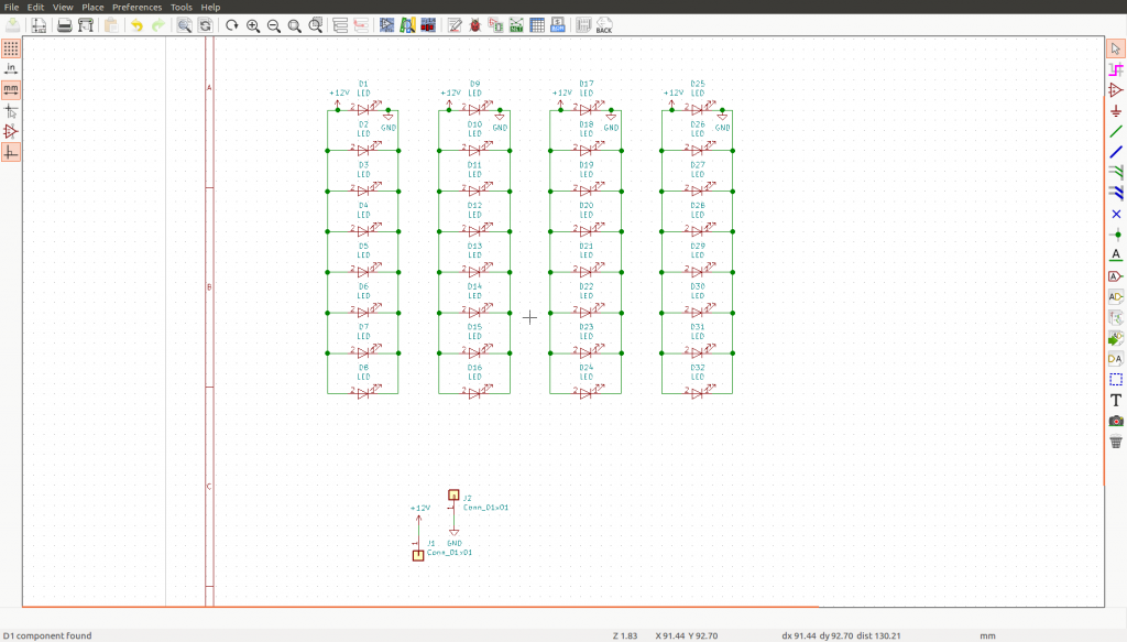
This is the placement that comes out of netlist read. I don’t see a pattern.
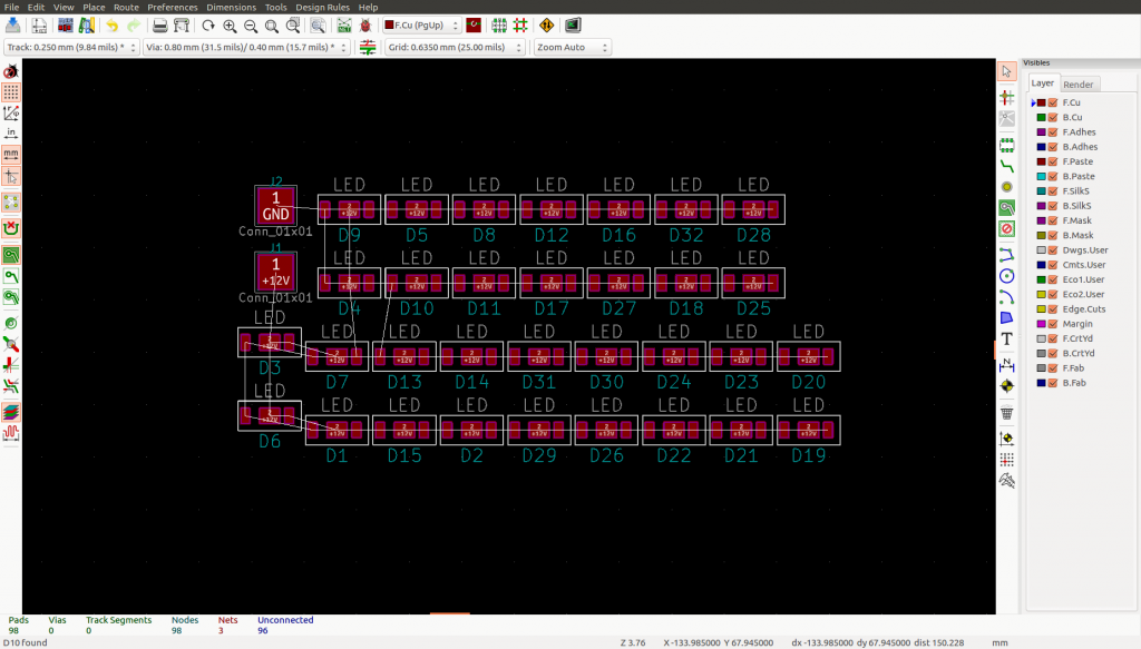
If I run this script from my github, I’ll get this:
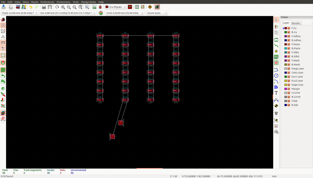
Not final, but it’s a sane starting point.
This short two minute video demonstrates. Not much to show, really:
How does it work? Pretty simple, actually. I parse the sch file for its device locations 1 and apply them to the layout. Most of it has been covered in my previous posts, but there are a couple of new things.
Where’s the schematic?
kicad has some infrastructure, called kiway, to pass information between applications. I suspect one could ask for a schematic file path there. I found it easy enough to ask pcbnew for the path to the current board and simply change the file extension.[code]
import pcbnew
board = pcbnew.GetBoard()
board_path = board.GetFileName()
sch_path = board_path.replace(“.kicad_pcb”, “.sch”)
[/code]
Getting location/transform from the sch
components look like this in the sch files:[code]
$Comp
L Device:LED D49
U 1 1 5A3B7115
P 6650 1500
F 0 “D49” H 6641 1716 50 0000 C CNN
F 1 “LED” H 6641 1625 50 0000 C CNN
F 2 “Miles:LED_5730” H 6650 1500 50 0001 C CNN
F 3 “~” H 6650 1500 50 0001 C CNN
1 6650 1500
1 0 0 -1
$EndComp
[/code]
I found a bit of documentation on the format on this website, but it’s not complicated. The things we need are:
- field 3 – “F 3” for the footprint name and location
- transform – “1 0 0 -1”. At first glance, this might seem a goofy way to represent it, but it’s just a matrix to multiply a point by.
- I also look at $Comp and $EndComp to ensure I’m not parsing locations from wire segments.
We have to do this because that information is not carried forward to pcbnew. I would like to see pcbnew support user properties. Block locations could be one such property but there are others. I think it makes more sense to define netclasses in the schematic and have that passed along.↩
Learnings from moving Kicad to wxPython 4.0
Kicad uses wx as its GUI platform and has a python interpreter built in. wxPython is used to bridge between wx and python. Kicad uses SWIG to expose its internal data structures to the Python world.
EDIT: the quote below mis-characterizes the person being quoted. See here for a good clarification of what he meant
I think strong scripting is one the best features many tools can provide but I fear that the kicad development team 1 doesn’t share in my enthusiasm. One of the reasons given why python support may be dropped is the need to migrate to wxPython 4.0, which is a rewrite of the previous 3.0.
https://lists.launchpad.net/kicad-developers/msg31672.html
I encourage everyone that finds the python interface to kicad valuable to post to the kicad developers list.Another thing, there will be no more wxPython releases. The project has been renamed to Phoenix and AFAIR nobody has tried to use it with KiCad. It may turn out that our SWIG work might be dropped/converted or we will stay stuck with wx3.0 forever.
So I tried running Kicad with the Phoenix version of wxPython. It seems to work, but it’s not quite ready to be used in released kicad. As far as I know, the more recent wx versions don’t do anything that breaks the wxPython 3.0 codebase.
The executive summary:
- Phoenix, as released, is not ready be embedded into applications. It’s usage thus far is as a plugin in Python. Kicad also uses python, but at the top level, it’s c++ main, not python.
- The only thing that’s missing is that the file src/wxpy_api.h isn’t copied from the source tree to Phoenix releases. See here.
- Phoenix uses SIP instead of SWIG to expose c++ to python. Kicad uses SWIG.
- In my kicad version using Phoenix, the wx stuff seems to work fine. I have some scripting that binds callbacks for mouse and key events. Seems to work.
- When installing Phoenix, you have to be careful of whether you have gtk2 or gtk3 on your system. Perhaps this was an issue before and I just accidentally installed the right one.
Needed code changes
There are only a handful changes needed to kicad’s code base to make it work with Phoenix. In the code snippets below, I give the original code, commented, followed by my replacement. Note that I didn’t try to do it “correctly”. I just wanted to get it to work.Here’s a diff file of the changes.
- CMakeLists.txt wants the wx version number to match the wxpython version. I just hacked it by hard coding the wxpython version to 4.0
#set( _wxpy_version “${wxWidgets_VERSION_MAJOR}.${wxWidgets_VERSION_MINOR}” )
set( _wxpy_version “4.0” )
[/code]
- CMakeLists.txt uses wxversions package to select the wx version. That subpackage is gone. Those wanting to have multiple wxpython versions installed should use virtual python environments.
#set( _py_cmd “import wxversion;print wxversion.checkInstalled(‘${_wxpy_version}’)” )
set( _py_cmd “import wx; import re; print(re.search(‘wxWidgets 3.0’, wx.wxWidgets_version) != None)”)
[/code]
- pcbnew/swig/python_scripting.cpp requires several changes.
[code]
//snprintf( cmd, sizeof(cmd), “import wxversion; wxversion.select(‘%s’)”, WXPYTHON_VERSION );
snprintf( cmd, sizeof(cmd), “import wx”);
[/code]
Next, wxPyCoreAPI_IMPORT() doesn’t exist anymore. I’m guessing that my change above to just import wx does the same thing.
Since Phoenix uses SIP instead of SWIG, the utilities used to convert between c++ and python have changed
[code]
//PyObject* arg = wxPyMake_wxObject( parent, false );
PyObject* arg = wxPyConstructObject(parent, “wxWindow”, false);
// unrelated code …
//bool success = wxPyConvertSwigPtr( result, (void**) &window, “wxWindow” );
bool success = wxPyConvertWrappedPtr(result, (void**) &window, “wxWindow”);
[/code]
- pcbnew/python/kicad_pyshell/__init__.py needs to initialize wx:App() and hold a pointer to it. I don’t know where this happened before; it’s not really new. I just added this code:
# there’s surely a better way to do this. I have to create
# and keep a pointer to the app object. If I don’t store this
# (otherwise unused) object, the garbage collector will delete
# it and other wx stuff will fail.
self.theApp = wx.App();
[/code]
- pcbnew/swig/python_scripting.h just needs to include the new interface file (which will hopefully be included in wxPython (4.0+ AKA Phoenix) releases)
// #include <wx/wxPython/wxPython.h>
#include <wxpy_api.h>
#include <wx/window.h>
[/code]
Installation details
One thing I found a little tricky was ensuring that the correct copies of everything are being sourced.gtk2 vs gtk3
I had gtk2 installed on my machine. The installation instructions example for wxPython is for gtk3. There is a gtk2 version, I just didn’t know to look for that difference. For pip base install, I used something like this:
[code]
pip install -U –pre \
-f https://wxpython.org/Phoenix/snapshot-builds/linux/gtk3/ubuntu-16.04 \
wxPython
[/code]
You can also build wxPython yourself. These instructions worked for me.
If you get an error like this
../src/common/object.cpp(251): assert "classTable->Get(m_className) == NULL" failed in Register(): Class "wxCommandEvent" already in RTTI table - have you used IMPLEMENT_DYNAMIC_CLASS() multiple times or linked some object file twice)?It means you have gtka based wx installed but wxPython wants a gtkb wx.
some prereqs
To get phoenix to install, I needed some package I hadn’t had before. This post was helpful, though I made these changes:- libtiff4 updated to libtiff5
- leave out libjpeg62-dev to avoid this error:
libjpeg-turbo8-dev : Conflicts: libjpeg62-dev but 1:6b2-2 is to be installed
[code]
sudo apt-get install libgl1-mesa-glx libglu1-mesa libgl1-mesa-dev libglu1-mesa-dev libgstreamer0.10-dev libgconf2-dev libsdl1.2-dev zlib1g-dev libtiff5-dev python-gst0.10-dev
[/code]
That’s it. Hope it was helpful.
Modify design rules from python
Even with the constructor exposed, the sequence of steps to get to it isn’t obvious.
[code]
import pcbnew
board = pcbnew.GetBoard()
ds = board.GetDesignSettings()
# ugly. exposes a public member not via an accessor method
nc = ds.m_NetClasses
foo = pcbnew.NETCLASSPTR(“foo”)
nc.Add(foo)
[/code]
The nc variable (NETCLASSPTR) has lots of useful get’er set’er functions, like SetClearance, SetTrackWidth. These are easy to find in the python window. Just type “foo.” and you should get a popup of available functions. You can also run the function “dir(foo)”
Pan, Zoom, Refresh from python in pcbnew
pcbnew.Refresh()
x = pcbnew.FromMM(10)
y = pcbnew.FromMM(10)
width  = pcbnew.FromMM(20)
height = pcbnew.FromMM(20)
pcbnew.WindowZoom(x, y, width, height)
Contributing to Kicad is painless
I initially searched and searched in pcbnew’s C code for python APIs like these. Eventually, I came to realize that they didn’t exist yet in pcbnew. So finally, I have my very first code contribution to an open source project. I’ve been paid to write software for many years but it’s all been in-house stuff. My professional environment was pretty loosey-goosey, with very few formal constraints. 1 Over the years, I’ve read lots of stories about how open source projects can be a pain to deal with. Lots of coding standards, lots of requirements,… lots of hoops to jump through.2 This was not my experience with proposing these code changes to Kicad. I read the developer wiki, and attempted with follow the directions. I mailed the patch file to the developer email list, along with an introduction of who I am and what I’m trying to accomplish. It was committed the same day. Wayne, the kicad project lead, was very welcoming and encouraging. Although there were a couple things I missed, he went ahead and did the tweaks and pushed the change. Next time, I’ll know. Most important to me, I’m excited to do more.This was mostly fine. On the one hand, a lot of bugs slipped through that shouldn’t have, but on the other, it meant that a lot of what we did was very much co-development/co-design with the users.↩
sometimes protection of empires, but probably also a lot critical code. I’d hope that mysql, Apache, linux kernel, g++,… are strict. Hopefully, they’ve also found ways to be welcoming. I don’t know. I guess it’s often the negative news that we remember., but probably also a lot critical code. I’d hope that mysql, Apache, linux kernel, g++,… are strict. Hopefully, they’ve also found ways to be welcoming. I don’t know. I guess it’s often the negative news that we remember.↩
Adding your own command buttons to the pcbnew GUI
Kicad has three rows of command buttons with predefined functionality. This post is about how to add your own button.
The sample code can be found here.
Perliminaries
Before getting into the code, there are a couple things that are weird about kicad/wxPython’s behavior1Getting proper aui pointers
The first thing is that if you simply open the python scripting window in pcbnew, find the top level window, and look for the command bars, you’ll likely get a pointer of type wxControl. That type doesn’t have the APIs needed to look at, amend, and change the command buttons. The real type of these is wx.aui.AuiToolBar but unless the pointer is cast correctly, you’re out of luck.After a bunch of poking around, running in the debugger, trying to recompile (unsuccessfully) wxPython with debug symbols turned on, I stumbled upon the easy answer. You have to do this before you run any of the wx scripting apis.
[code]
import wx
import wx.aui # this is the key one
[/code]
After running these, you’ll get the correct pointer types. 2
Getting a proper WxApp pointer
The second funny thing isn’t really needed to add a button, but it’s super helpful in looking at the structure of the GUI yourself. In this post, I’m not just trying to help you add a button in a specific place, but rather to help you learn more about how pcbnew is put together. With this understanding you’ll hopefully be able to do even more.When you first open the python interpreter in pcbnew, if you ask for the wxApp pointer, you’ll get a pointer of type wxEvtHandler. While this is correct, it’s incomplete and also unhelpful if you need a wxApp pointer. If you do this, wx.GetApp() will return a usable wxApp pointer3
[code]
import wx
wx.App()
[/code]
Note that if you do this more than once in a given session, it’ll crash pcbnew.4
So why do we care? Well, if you have a proper wxApp pointer you can do this (remember, only one call to wx.App() per session):
[code]
import wx
wx.App()
import wx.aui
import wx.lib.inspection
wx.lib.inspection.InspectionTool().Show()
[/code]
Which will give you a Widget Inspection Tool window like the one below. It enables you to click on different parts of the pcbnew GUI and see what’s what. Note that it doesn’t give me information about the individual buttons. It’s a helpful learning/debug aid nonetheless.

So let’s add a button
There are a couple things you need to add a button- The toolbar you want to add the button to (top, left, or right)
- A callback function to be called when the button is clicked
- A picture/bitmap to use as your button’s icon.
Getting the toolbar to add to
To lookup the toolbar window, you start by finding the main pcbnew window and then asking it for one of its children by id number. How do you know the number? The current, bad, answer is to either use the window inspector I mentioned earlier in this post or for me to tell you.5 Here are the numbers:(this has been fixed. you can now use pcbnew.ID_H_TOOLBAR, pcbnew.ID_AUX_TOOLBAR and so on.)
- 6038 is the value that H_TOOLBAR from kicad/include/id.h happens to get. It’s the one on the top with buttons like “new board”, “open existing board”
- 6041 is AUX_TOOLBAR. That’s the second row of stuff in the pcbnew gui. It contains things like track width, via size, grid
- 6039 is V_TOOLBAR, the right commands window. zoom to selection, highlight net.
- 6040 is OPT_TOOLBAR, the left commands window. disable drc, hide grid, display polar
import pcbnew
import wx
import wx.aui
def findPcbnewWindow():
windows = wx.GetTopLevelWindows()
pcbnew = [w for w in windows if w.GetTitle() == “Pcbnew”]
if len(pcbnew) != 1:
raise Exception(“Cannot find pcbnew window from title matching!”)
return pcbnew[0]
pcbwin = findPcbnewWindow()
top_tb = pcbwin.FindWindowById(6038)
[/code]
Callback function
This one’s easy. It’s just a function that takes the event as an argument. If you print from this function, the output will appear in the terminal used to invoke pcbnew, not the python window. The event will be of type wx.CommandEvent which is useful to know if you want to have one callback for a variety of buttons.[code]
def MyButtonsCallback(event):
# when called as a callback, the output of this print
# will appear in your xterm or wherever you invoked pcbnew.
print(“got a click on my new button {}”.format(str(event)))
[/code]
icon image
If you were to look in the kicad source code for bitmaps_png/CMakeLists.txt you’d find this:The rest of that file handles automagic conversion from svg files into a format that can be consumed by the kicad code. Things are easier for us. You just need a 26×26 image file. In this example, I use png format, but you can use any format listed here on the wxPython page# Plan for three sizes of bitmaps:
# SMALL – for menus – 16 x 16
# MID – for toolbars – 26 x 26
# BIG – for program icons – 48 x 48
[code]
# assuming you’re creating your button from a script, one logical place to keep
# the image is in the same directory. Here’s a snippet for how to get the
# path of the script.
import inspect
import os
filename = inspect.getframeinfo(inspect.currentframe()).filename
path = os.path.dirname(os.path.abspath(filename))
# here we actually load the icon file
bm = wx.Bitmap(path + ‘/hello.png’, wx.BITMAP_TYPE_PNG)
[/code]
Putting it all together
Now we have top_tb holding the toolbar window we want to add to, bm holding a bitmap pointer, and MyButtonsCallback to do the work. Now we just need to add a new tool button, bind it to the callback and tell the system to make it real.[code]
itemid = wx.NewId()
top_tb.AddTool(itemid, “mybutton”, bm, “this is my button”, wx.ITEM_NORMAL)
top_tb.Bind(wx.EVT_TOOL, MyButtonsCallback, id=itemid)
top_tb.Realize()
[/code]
And that’s it. Hope you enjoyed the post. Please comment. Again, the sample code can be found here.

Things are only weird if you don’t know the explanation. In this case, I can guess at the reasons, but I don’t know for sure.↩
if you already have the pointer with the wrong type, subsequent searches for windows will yield the same unhelpful type. My theory on why this is so is a matter of caching (why it persists) and swig symbol tables. Before you do import wx.aui, these types are not yet known to python and swig, so they return a type that is known. wxControl↩
probably incorrect, but usable for what I’m about to talk about.↩
again, this is a bad solution, but it’s only needed for debugging and learning about pcbnew’s structure.↩
The better answer is for the kicad enum that holds these number to be exposed in python. Easy to add, but it’s not there now. that holds these number to be exposed in python. Easy to add, but it’s not there now. ↩