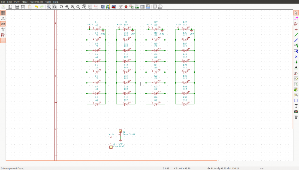
For example, say I have a schematic like this (click to enlarge). The leds are annotated D1-8 down the first column.
This is the placement that comes out of netlist read. I don’t see a pattern.

If I run this script from my github, I’ll get this:

Not final, but it’s a sane starting point.
This short two minute video demonstrates. Not much to show, really:
How does it work? Pretty simple, actually. I parse the sch file for its device locations 1 and apply them to the layout. Most of it has been covered in my previous posts, but there are a couple of new things.
Where’s the schematic?
kicad has some infrastructure, called kiway, to pass information between applications. I suspect one could ask for a schematic file path there. I found it easy enough to ask pcbnew for the path to the current board and simply change the file extension.[code]
import pcbnew
board = pcbnew.GetBoard()
board_path = board.GetFileName()
sch_path = board_path.replace(“.kicad_pcb”, “.sch”)
[/code]
Getting location/transform from the sch
components look like this in the sch files:[code]
$Comp
L Device:LED D49
U 1 1 5A3B7115
P 6650 1500
F 0 “D49” H 6641 1716 50 0000 C CNN
F 1 “LED” H 6641 1625 50 0000 C CNN
F 2 “Miles:LED_5730” H 6650 1500 50 0001 C CNN
F 3 “~” H 6650 1500 50 0001 C CNN
1 6650 1500
1 0 0 -1
$EndComp
[/code]
I found a bit of documentation on the format on this website, but it’s not complicated. The things we need are:
- field 3 – “F 3” for the footprint name and location
- transform – “1 0 0 -1”. At first glance, this might seem a goofy way to represent it, but it’s just a matrix to multiply a point by.
- I also look at $Comp and $EndComp to ensure I’m not parsing locations from wire segments.
Copying schematic placement to layout
We have to do this because that information is not carried forward to pcbnew. I would like to see pcbnew support user properties. Block locations could be one such property but there are others. I think it makes more sense to define netclasses in the schematic and have that passed along.↩