Panelizing Kicad gerbers

When I google for kicad and panelize, a top link is this one which talks about this panelizer written by Stijn Kuipers. The instructions given there are almost enough for me
I had two difficulties with the panelizer, but once I got beyond those, the process is quite easy. The troubles for me where:
  • I’m a linux guy. The released version doesn’t run under mono. There’s a side version that works well
  • I’m a kicad guy and the hackaday tutorial, while mentioning kicad, seems targeted at Eagle people. This is also easy to deal with if you know a couple key pieces of information.
Edit Dec 29, 2017: I’ve added a section simple panelizing directly in Kicad. Also, I added a comment on pcbshopper in the rant

Running on linux

When I run the released panelizer via the latest mono I could find for linux, I ran into the issue reported here, ie I get a message that contains this:
System.ArgumentException: XOR data length expected 
There’s a bunch of discussion in the issue, but the short answer is to use a compile that runesoeknudsen attached to the ticket. The compiled working version can be downloaded here. It hasn’t given me any trouble on ubuntu 16.04 and 5.4.1.6, but I’m guessing any mono will be fine.

Kicad related issues

The other issue I had was that the tutorial was written from the perspective of a non-kicad user. There are a couple things you have to watch for:
  • the panelizer is looking for a particular file extension for drilled holes
  • the panelizer is looking for a particular file extension for the board outline
  • and it is looking for particular file extensions for the layer files.
Notice any common themes? It’s trivial, actually, but… most things aren’t hard… if you know how to do them. 1.

Drill file

Generate the drill file as normal. Just rename it to .txt. If you don’t do this, you’ll get a merged drl file and a merged txt file. the drl file will contain your original holes, properly translated to the panelized positions. The txt file will contain the holes needed for the break away tabs.

Board outline

This a simple matter of renaming the gm1 file to gko.

The layer files

You have to use the kicad plot option “Use Protel filename extensions”. Kicad gives a help message “this is no longer recommended”, which misled me for a bit. In this case, I recommend it.
 

Simple panelizing directly in Kicad

If you start pcbnew directly, 2 you’ll get the “append board” command in the file menu. So starting with a new board, append each design you want.
Note that nets with the same net will get merged, so if you delete GND, all of ground will be deleted. You may also get opens reported.
You might find my gen_border script useful3, which will shrink a rectangular boarder around your design. It’ll also add a power and/or gnd zone on the same boundary.

A rant

The rest of this post adds nothing about how to panelize. Instead I want to rant a little.
There are a bunch of services out there that offer cheap pcb fabrication for 10cmx10cm 2 layer boards. If you submit a set of gerbers that looks like multiple designs, they won’t make it for you. They want more money.
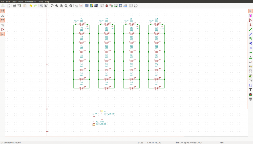
I recently did two small LED boards. They’re pretty small, so I put two of one and one of the other in a design and sent it off. denied.
Why?
My design has very few holes. The outline is not that complex, even with the added tabs. What’s the problem? I’m paying for 10×10 and 2 layers. I’m not ask for anything beyond that.
What’s the cheapest service that won’t hassle you for including multiple designs on one board? I am aware of pcbshopper.com. The problem is that even if you enter something other than 1 in the multiple designs field, the returned links won’t allow multiple designs. Also, dirtypcbs and seeed studio are said to be panelize friendly, but with shipping, you might as well buy multiple designs from a cheaper vendor. I think all this is a sign that I’m too cheap. I’m racing to the bottom.
 
 
Panelizing Kicad gerbers

  1. my corollary to this is: “nothing is wierd… once you know the explanation for it.

  2. ie, close the kicad project manager and just open pcbnew,

  3. I need to plugin’ify it so it can be run from the “external plugins” menu

Copying schematic placement to layout

When importing a netlist to pcbnew, I get what appears to be a random placement. While the schematic placement is usually not a final placement for layout, it’s surely better than random.
For example, say I have a schematic like this (click to enlarge). The leds are annotated D1-8 down the first column.
This is the placement that comes out of netlist read. I don’t see a pattern.

If I run this script from my github, I’ll get this:

Not final, but it’s a sane starting point.
This short two minute video demonstrates. Not much to show, really:
 

How does it work? Pretty simple, actually. I parse the sch file for its device locations 1 and apply them to the layout. Most of it has been covered in my previous posts, but there are a couple of new things.

Where’s the schematic?

kicad has some infrastructure, called kiway, to pass information between applications. I suspect one could ask for a schematic file path there. I found it easy enough to ask pcbnew for the path to the current board and simply change the file extension.
[code]
import pcbnew
board = pcbnew.GetBoard()
board_path = board.GetFileName()
sch_path = board_path.replace(“.kicad_pcb”, “.sch”)
[/code]

Getting location/transform from the sch

components look like this in the sch files:
[code]
$Comp
L Device:LED D49
U 1 1 5A3B7115
P 6650 1500
F 0 “D49” H 6641 1716 50 0000 C CNN
F 1 “LED” H 6641 1625 50 0000 C CNN
F 2 “Miles:LED_5730” H 6650 1500 50 0001 C CNN
F 3 “~” H 6650 1500 50 0001 C CNN
1 6650 1500
1 0 0 -1
$EndComp
[/code]
I found a bit of documentation on the format on this website, but it’s not complicated. The things we need are:
  • field 3 – “F 3” for the footprint name and location
  • transform – “1 0 0 -1”. At first glance, this might seem a goofy way to represent it, but it’s just a matrix to multiply a point by.
  • I also look at $Comp and $EndComp to ensure I’m not parsing locations from wire segments.
That’s it, really. Just have to remember that eeschema stores coordinates in thousandths of an inch and pcbnew uses millionths of a mm.
Copying schematic placement to layout

  1. We have to do this because that information is not carried forward to pcbnew. I would like to see pcbnew support user properties. Block locations could be one such property but there are others. I think it makes more sense to define netclasses in the schematic and have that passed along.